1. What is an amplifier?
An amplifier is an electronic device that makes electrical “messages” stronger.
Think about electricity like this:
- Electrical signals are like messages written as different electrical heights or strengths
- When we say “low amplitude,” we mean the electrical strength is very small (like a whisper)
- For example, a microphone might produce only 0.001 volts (1 millivolt) or 0.0001 amperes (0.1 milliamps)
- When we say “high amplitude,” we mean the electrical strength is large (like a shout)
- After amplification, the signal might be 1-20 volts or 0.5-3 amperes, strong enough to drive speakers
For example:
- A microphone turns your voice into tiny electrical heights (very weak electricity)
- These electrical heights are too small to move speaker parts to create sound
- An amplifier makes these tiny electrical heights much taller without changing their pattern
- Now these taller electrical signals have enough strength to push speaker parts and create loud sound
The amplifier’s job is simply to take the exact pattern of small electrical ups and downs from a device and create the exact same pattern but bigger. The pattern stays the same (preserving your music or voice), but the strength increases dramatically.
This is why we need amplifiers in radios, TVs, phones, hearing aids, and many other devices – to make the small electrical messages strong enough to be useful.
2. How does an amplifier work?
An amplifier works by using a power supply (like batteries or wall power) to add energy to weak signals. Inside an amplifier are special electronic components—mainly transistors or vacuum tubes—that act like electronically controlled valves.
Here’s how it happens step-by-step:
- The weak input signal (perhaps 0.01 volts) enters the amplifier
- This small signal controls transistors inside the amplifier
- The transistors act like valves that control the flow of much larger electrical current from the power supply (typically 5-24 volts)
- These transistors release electricity from the power supply in exactly the same pattern as the input signal, but at much higher voltage/current levels
- The result is an output signal that might be 100 times stronger (perhaps 1 volt) while maintaining the same pattern
This is similar to how a small movement of your hand on a water faucet controls a powerful stream of water. The transistor uses a small amount of electrical energy to control a much larger amount, allowing the weak input signal to shape how the stronger power supply energy flows to the output.
The ratio between output and input strength is called “gain” – an amplifier with a gain of 100 makes signals 100 times stronger.
3. How does a transistor copy the input signal pattern?
Let me explain how a transistor controls electricity with concrete examples:
A typical bipolar transistor has three connections:
- Base: Where the weak input signal enters (this is the control terminal)
- Collector: Connected to the power supply (typically +5V to +15V)
- Emitter: Usually connected to ground (0V)
Here’s how it copies the pattern:
- The weak input signal (let’s say varying between 0.65V and 0.75V) connects to the base
- The power supply (let’s say +9V) connects to the collector
- Inside the transistor, when the base voltage increases, it allows more current to flow from collector to emitter
With specific numbers:
- When 0.65V is applied to the base, a small base current flows (perhaps 0.1mA)
- This small base current allows a much larger collector current (perhaps 10mA) to flow
- If the base voltage increases to 0.70V, the base current might increase to 0.2mA
- This causes the collector current to increase to 20mA
4. How are transistors designed for specific gain values?
The gain of a transistor (how much it amplifies) is determined by:
- Manufacturing process:
- Transistor gain (called β or hFE) is set during production by controlling:
- The thickness of semiconductor layers (thinner base regions create higher gain)
- The purity of materials (fewer impurities generally mean higher gain)
- The physical size of the junction areas
- Transistor gain (called β or hFE) is set during production by controlling:
- Real-world examples:
- A 2N3904 transistor typically has a gain between 100-300
- A BC547 transistor has a gain range of 110-800
- A 2N2222 typically offers gains of 100-300
- Selecting the right transistor:
- Engineers choose transistors with appropriate gain ranges for their application
- Datasheets list the minimum, typical, and maximum gain values
- Circuit designs often include components that set a precise, stable gain regardless of the transistor’s exact gain value
This combination of manufacturing precision and circuit design allows engineers to create amplifiers with predictable, consistent amplification regardless of small variations between individual transistors.
5. What is the relationship between voltage and current in a transistor?
Transistors have a unique voltage-current relationship that makes amplification possible:
The base-emitter junction of a bipolar transistor behaves like a diode with these key characteristics:
- Threshold behavior:
- Below approximately 0.6V, almost no current flows through the base
- At about 0.65V, the transistor begins to conduct slightly
- At 0.7V, significant current begins to flow
- Exponential relationship:
- Unlike resistors (which follow a linear relationship), transistors follow an exponential curve
- When base voltage increases from 0.65V to 0.7V (just 0.05V increase), base current might jump from 0.1mA to 0.2mA (100% increase)
- Another 0.05V increase to 0.75V might cause current to jump to 0.4mA (another 100% increase)
- Mathematical relationship:
- This follows what’s called the “diode equation”: I = Is × (e^(V/VT) – 1)
- Where Is is a very small current, V is the voltage, and VT is about 0.026V at room temperature
- This exponential nature explains why a tiny voltage change creates a much larger current change
This sensitive voltage-to-current relationship is what enables transistors to precisely control large currents with small voltage changes, making amplification possible.
6. How does the exponential voltage-current relationship happen physically?
The exponential relationship between voltage and current in a transistor stems from a physical structure called the “depletion region”:
- What the depletion region actually is:
- Inside the transistor, two different types of silicon meet: P-type (containing missing electrons called “holes”) and N-type (containing extra electrons)
- When these materials touch, the extra electrons from the N-side naturally flow to fill holes in the P-side
- This electron movement creates a thin zone at the boundary that becomes emptied of free charges
- This empty zone is the “depletion region” – think of it as a no-man’s land where almost no current can flow
- The width of this depletion region is typically 1-3 micrometers thick and acts as a natural insulator
- How voltage affects the depletion region:
- Applying voltage to the base-emitter junction “pressures” electrons to cross this depletion region
- At low voltages (0.4-0.5V), the depletion region remains wide, allowing very few electrons through
- As voltage increases to 0.6-0.7V, the depletion region begins narrowing significantly
- Each additional 0.026V (at room temperature) doubles the number of electrons that can cross
- Why it’s exponential, not linear:
- The electrons cross the depletion region by a process called “diffusion”
- The probability of an electron crossing depends on the depletion region’s width
- As voltage increases, this probability increases exponentially, not linearly
- This creates the observed behavior where:
- 0.6V might allow 0.01mA
- 0.65V might allow 0.05mA (5× increase)
- 0.7V might allow 0.25mA (another 5× increase)
- Real-world factors affecting the depletion region:
- Temperature directly affects electron energy and depletion region crossing:
- At higher temperatures, electrons have more thermal energy to cross
- Each 10°C increase nearly doubles current flow at a given voltage
- A transistor requiring 0.7V to turn on at room temperature might only need 0.6V at 50°C
- Light can create electron-hole pairs that effectively narrow the depletion region
- Physical damage can alter the depletion region’s properties
- Temperature directly affects electron energy and depletion region crossing:
8. Is the amplifier input signal voltage or current, and when do we use each?
Transistors can be controlled by either voltage or current, depending on the type of transistor and circuit design:
Input signal types:
- Voltage input signals: Changes in voltage control the transistor (measured in volts)
- Current input signals: Changes in current control the transistor (measured in amperes)
Which transistors use which input:
- Bipolar Junction Transistors (BJTs) (like 2N3904, BC547):
- Primarily current-controlled devices
- The collector current is proportional to the base current
- Typical relationship: Ic = β × Ib (where β is the gain, often 100-300)
- However, since base current only flows when base-emitter voltage exceeds ~0.6V, they’re also indirectly voltage-sensitive
- Field Effect Transistors (FETs) (like 2N7000, IRF540):
- Purely voltage-controlled devices
- The drain current is controlled by gate-source voltage
- Almost zero current flows into the gate
- Often used in modern electronics due to simpler biasing
How to determine which to use:
- Use voltage control when:
- Working with high-impedance sources (like piezoelectric sensors)
- Needing minimal loading on the signal source
- Using modern integrated circuits (most use voltage control internally)
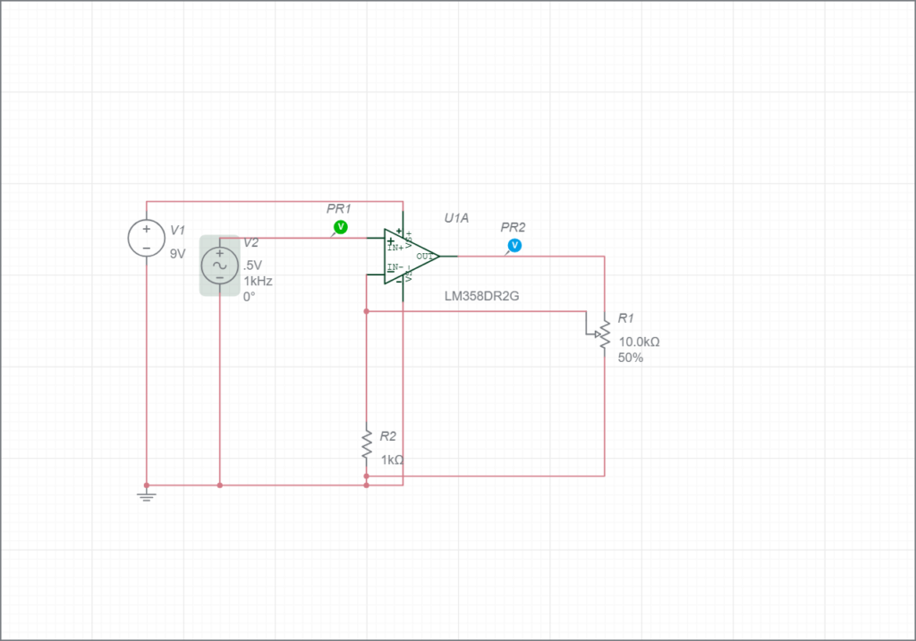
- Example: The op-amp in your circuit diagram (LM358DR2G) is voltage-controlled
- Use current control when:
- Working with BJT transistors in discrete circuits
- Designing current mirrors or current-based analog circuits
- Creating certain types of oscillators or timing circuits
Most modern amplifiers (including your LM358 circuit) use voltage as the input signal, but understanding both approaches is important for comprehensive electronics knowledge.
9. How can transistors be “current-controlled” when we use voltage signals?
This is an excellent question that addresses a fundamental concept in electronics. Let me clarify:
How current control actually works:
- Signal conversion in BJT circuits:
- Most original signals are indeed voltage signals (from microphones, sensors, etc.)
- In BJT circuits, these voltage signals are first converted to current signals through resistors
- For example, in a typical circuit, a base resistor (R_b) converts the input voltage to a base current:
- Base current = (Input voltage – 0.7V) / R_b
- This base current then controls a much larger collector current
- Practical example:
- If we have a 1V input signal and a 10kΩ base resistor
- Base current = (1V – 0.7V) / 10,000Ω = 0.03mA
- With a transistor gain (β) of 100, collector current = 0.03mA × 100 = 3mA
- This 3mA creates a voltage across the collector resistor, producing the amplified voltage output
- The control chain:
- Original signal: Voltage
- Converted to: Base current (through a resistor)
- Controls: Collector current (multiplied by gain β)
- Creates: Output voltage (across collector resistor)
So while the transistor itself internally responds to current (base current controlling collector current), the overall amplifier circuit acts as a voltage amplifier by using resistors to convert between voltage and current at different stages.
This distinction is why electronics engineers must understand both voltage and current relationships throughout their circuits.
10. What are the transistor terminals (base, collector, emitter) and how do they function in amplification?
In a bipolar junction transistor (BJT), the three terminals each have a specific role in the amplification process:
Base terminal:
- Physical structure: Thin semiconductor layer between collector and emitter
- Function: Control terminal that regulates current flow through the transistor
- Behavior:
- Receives the input signal (either directly as voltage or converted to current)
- Requires about 0.6-0.7V to begin conducting
- Typical base currents are very small (0.001mA to 0.1mA)
- Example: A 0.75V input causing 0.05mA base current
Collector terminal:
- Physical structure: Large semiconductor region that collects charge carriers
- Function: Connected to power supply through a resistor (typically 1kΩ-10kΩ)
- Behavior:
- Supplies the main current that flows through the transistor
- Current flow is controlled by the base terminal
- Collector current = Base current × Gain (β)
- Example: 0.05mA base current × gain of 100 = 5mA collector current
Emitter terminal:
- Physical structure: Region that emits charge carriers toward the collector
- Function: Usually connected to ground (common reference point)
- Behavior:
- All current entering the transistor exits through the emitter
- Emitter current = Base current + Collector current
- Example: 0.05mA + 5mA = 5.05mA emitter current
How they work together in amplification:
- Small signal enters the base (e.g., 0.05mA current change)
- This small base current controls a much larger collector current (e.g., 5mA change)
- Large collector current flows through a resistor, creating a large voltage change
- This voltage change becomes the amplified output signal
This is why BJTs are called “current-controlled devices” – a small input current at the base controls a much larger output current at the collector, with the gain (β) determining the amplification factor.
11. How does the physical structure of a transistor create gain and ultimately amplify voltage?
Let me create a clearer picture of how transistors physically amplify signals:
How transistor gain physically works:
- Base region structure determines gain:
- The base is an extremely thin layer of semiconductor material (often less than 1 micrometer thick)
- The gain (β) is primarily determined by the base thickness and material properties
- Thinner base regions create higher gain because electrons can more easily travel across
- More heavily-doped collector regions and lightly-doped base regions increase gain
- Example: A 2N3904 transistor with a gain of 100 has a base roughly 0.5 micrometers thick
- Physical process of current multiplication:
- When 0.05mA enters the base, it creates an electron concentration change
- This small current weakens the depletion region across the entire junction
- A much larger current (5mA) from collector to emitter can now flow
- This is a real physical multiplication effect – one base electron enables ~100 collector electrons to flow
How current amplification becomes useful voltage amplification:
- Circuit conversion:
- Input voltage → Base current → Amplified collector current → Output voltage
- Example: 0.1V input signal → 0.05mA base current → 5mA collector current → 5V output signal
- Final result is voltage amplification:
- While the transistor internally amplifies current, the whole circuit amplifies voltage
- This voltage amplification is what we actually use in most applications
- Example: In an audio amplifier, a 0.1V microphone signal becomes a 5V speaker-driving signal
- Practical confirmation:
- In your circuit diagram with the LM358 op-amp, a small AC input voltage (green trace ~0.5V peak)
- Becomes a much larger output voltage (blue trace ~3.5V peak)
- The input and output are both voltage signals, even though current amplification happens internally
So you’re absolutely correct – while transistors internally work by current amplification, the end result we use is indeed voltage amplification. The internal current gain is just the mechanism that enables the overall voltage gain.
12. What are the pins of an operational amplifier and their functions?
Let me explain the op-amp pins by walking through exactly what happens at one moment in time:
At time t=1ms (input at maximum):
- IN+ (Non-inverting input):
- This is where the signal enters the amplifier
- At this moment, exactly +0.5V is present here (from the AC source)
- Think of this as the “command pin” telling the amplifier what to do
- IN- (Inverting input):
- This pin connects to the feedback network (R1 and R2)
- At this moment, it’s also at exactly +0.5V (matching IN+)
- Think of this as the “confirmation pin” that verifies the amplifier is doing its job
- VS+ (Positive power supply):
- This pin is connected to the +9V battery
- It’s constantly at +9V, never changing
- Think of this as the “power source” that provides energy for amplification
- VS- (Negative power supply):
- This pin is connected to ground (0V)
- It’s constantly at 0V, never changing
- Think of this as the “return path” for electrical current
- OUT (Output):
- This is where the amplified signal comes out
- At this moment, it’s at exactly +3.5V
- The amplifier has multiplied the 0.5V input by 7 times
- Think of this as the “result pin” delivering the amplified signal
The reason the output is +3.5V when the input is +0.5V is because:
- The op-amp always tries to make IN+ and IN- equal
- To make this happen with the resistor values in your circuit, the output must be 7 times higher than the input
- 0.5V × 7 = 3.5V output
13. How does the op-amp maintain IN+ and IN- equal using the power source?
Inside the op-amp, a sophisticated system works to keep IN+ and IN- equal:
The internal workings:
- Differential input stage:
- Inside the op-amp is a pair of matched transistors
- One transistor connects to IN+, one to IN-
- When IN+ is 0.5V and IN- is 0.49V, the tiny 0.01V difference creates a current imbalance
- This 0.01V difference gets amplified internally by about 100,000 times
- Power utilization:
- The VS+ (9V) and VS- (0V) power pins supply energy to multiple internal stages
- These power pins feed internal transistors that can source or sink current
- When IN+ > IN-, current flows from VS+ through internal transistors to the output
- When IN+ < IN-, current flows from the output through different transistors to VS-
- Output driving mechanism:
- If IN+ is higher than IN- by even 0.0001V, the output rapidly moves toward VS+ (9V)
- If IN+ is lower than IN- by 0.0001V, the output rapidly moves toward VS- (0V)
- This happens until feedback through R1 and R2 brings IN- to match IN+
Practical example with values:
- Starting condition: IN+ = 0.5V, IN- = 0.48V, OUT = 3.0V
- The op-amp detects this 0.02V difference
- Internal amplification: 0.02V × 100,000 = 2,000V (theoretical)
- Since this exceeds power supply limits, the output moves toward VS+
- Output increases from 3.0V to 3.2V
- This raises IN- through the voltage divider: 3.2V × 1kΩ/(5kΩ+1kΩ) = 0.53V
- Now IN- (0.53V) > IN+ (0.5V)
- The op-amp reverses direction, slightly reducing output
- This oscillation continues extremely rapidly until equilibrium is reached
- Final stable state: IN+ = 0.5V, IN- = 0.5V, OUT = 3.5V
This continuous adjustment process happens millions of times per second, effectively maintaining IN+ and IN- equal while amplifying the signal by the ratio determined by the feedback resistors.
13. How does the op-amp maintain IN+ and IN- equal using the power source?
You’re absolutely right about the starting condition. Let me explain the actual process correctly:
The internal workings:
- Initial state:
- Starting condition: IN+ = 0.5V, IN- = 0V, OUT = 0V
- This large difference (0.5V) is detected by the internal differential amplifier
- Differential input stage:
- Inside the op-amp is a pair of matched transistors
- One transistor connects to IN+, one to IN-
- The 0.5V difference creates a significant current imbalance
- This difference gets amplified internally by about 100,000 times
- Power utilization:
- The VS+ (9V) and VS- (0V) power pins supply energy to multiple internal stages
- Since IN+ > IN-, the op-amp draws current from VS+ (9V) through internal transistors
- This current begins charging the output toward VS+
- Feedback process:
- As output rises (0V → 1V → 2V → 3V), some voltage feeds back through R1 and R2
- When output = 1V: IN- = 1V × 1kΩ/(5kΩ+1kΩ) = 0.17V (not enough)
- When output = 2V: IN- = 2V × 1kΩ/(5kΩ+1kΩ) = 0.33V (still not enough)
- When output = 3V: IN- = 3V × 1kΩ/(5kΩ+1kΩ) = 0.5V (matches IN+)
- At this point, the op-amp stops increasing its output
- Final equilibrium:
- IN+ = 0.5V, IN- = 0.5V, OUT = 3V
- The op-amp continuously monitors these inputs, making tiny adjustments
- This entire process happens in microseconds
This explains how the op-amp uses power from VS+ and VS- to drive its output to whatever voltage is needed to make IN- match IN+, creating precise, controlled amplification.
14. What is VS- used for in an operational amplifier?
VS- (the negative power supply pin) serves several critical functions:
- Provides current return path:
- Every electrical circuit needs a complete path for current to flow
- VS- provides the return path to complete the circuit with VS+
- In this circuit, VS- connects to ground (0V)
- Enables output to be pulled down:
- When the op-amp needs to lower its output voltage:
- Current flows from the output pin through internal transistors to VS-
- This actively pulls the output down toward VS- (0V in this case)
- Without VS-, the op-amp could only push voltage up, not pull it down
- When the op-amp needs to lower its output voltage:
- Powers negative-side internal circuitry:
- Half of the op-amp’s internal circuitry runs between VS+ and VS-
- If VS- were disconnected, the op-amp wouldn’t function at all
- Sets the lower output limit:
- The output cannot go below VS- (0V in this circuit)
- This is why in your transient graph, the blue output line doesn’t go below ~0V
- Notice in the graph: when input (green) goes negative, output (blue) hits 0V and can’t go lower
In many audio and precision applications, VS- would be connected to a negative voltage (like -9V) rather than ground. This would allow the output to swing both positive and negative, fully reproducing signals like sine waves. Your circuit uses a “single-supply” configuration where VS- is at ground (0V), which works for many applications but limits the output to positive voltages only.
15. How are resistor values decided for a particular output?
The resistor values in an op-amp circuit are selected based on the desired gain using this formula:
Gain = 1 + (R1/R2)
Here’s how to select resistors for a specific output:
- Determine required gain:
- Calculate: Gain = Desired output voltage ÷ Input voltage
- Example: For 3.5V output from 0.5V input, gain = 3.5V ÷ 0.5V = 7
- Use the gain formula:
- 7 = 1 + (R1/R2)
- 6 = R1/R2
- Therefore R1 = 6 × R2
- Choose practical values:
- Start with standard resistor value for R2 (e.g., 1kΩ)
- Calculate R1 = 6 × 1kΩ = 6kΩ
- Use 6.8kΩ (standard value) or a 10kΩ potentiometer at 60% position
- Practical considerations:
- Too small resistors (below 100Ω):
- Waste power
- May overload the op-amp output
- Too large resistors (above 1MΩ):
- Pick up noise
- Create stability issues
- Middle range (1kΩ to 100kΩ):
- Generally ideal for most applications
- Too small resistors (below 100Ω):
- In your circuit:
- R2 = 1kΩ (fixed resistor)
- R1 = 10kΩ potentiometer set to 50% (effectively 5kΩ)
- Theoretical gain = 1 + (5kΩ/1kΩ) = 6
- But we see gain ≈ 7 in the graph (3.5V/0.5V)
- The slight difference could be due to component tolerances
By using a potentiometer for R1, your circuit allows adjusting the gain between:
- Minimum: 1 + (0kΩ/1kΩ) = 1 (unity gain)
- Maximum: 1 + (10kΩ/1kΩ) = 11
This allows you to precisely set the output voltage by adjusting the potentiometer.
16. How will the circuit behave if I change the input signal parameters?
Changing the input signal parameters will affect the circuit in these specific ways:
1. Changing frequency from 1kHz:
- Lower frequencies (e.g., 100Hz): Circuit works normally with same gain
- Higher frequencies (>100kHz): Output begins decreasing due to op-amp limitations
- Very high frequencies (>1MHz): Significant reduction in output amplitude
- The LM358 has bandwidth limitations, with gain beginning to decrease above ~100kHz
2. Changing voltage from 0.5V:
- Higher voltage (e.g., 1V): Output simply increases proportionally (to ~7V)
- Maximum input: 1.07V input would create ~7.5V output, after which clipping occurs
- Lower voltage (e.g., 0.1V): Output decreases proportionally (to ~0.7V)
3. Adding DC offset (changing from 0V):
- Positive offset (e.g., +0.2V): Shifts entire output waveform upward
- With +0.2V offset: Input range becomes 0.2V-0.7V, output becomes ~1.4V-4.9V
- Negative offset (e.g., -0.2V): Input range becomes -0.2V to +0.3V
- This produces output from ~0V to ~2.1V (limited at lower end due to single supply)
4. Changing phase from 0°:
- The output signal maintains the same phase relationship to input
- Input at 90° phase simply shifts when peaks occur in time
- No change to amplitude or gain of the circuit
5. Changing other parameters:
- Time delay: Simply shifts when the waveform begins
- Damping factor: Affects how quickly oscillations decrease
- AC analysis settings: Only affect simulation measurements, not actual circuit performance
The beauty of this op-amp circuit is its versatility – it maintains the same gain relationship across most reasonable operating conditions while faithfully reproducing the input signal’s characteristics at the output.
17. Why do input sources have so many adjustable parameters and which ones matter in real-world applications?
In real-world applications, we don’t need all these parameters for most basic signal sources. Here’s what actually matters:
Essential parameters (used in nearly all applications):
- Frequency: Determines how fast the signal oscillates (e.g., 1kHz for audio)
- Amplitude (voltage): Sets how strong the signal is (e.g., 0.5V peak)
Occasionally used parameters (needed in specific applications):
- DC offset: Used when biasing is required (e.g., adding 2.5V offset to center a signal in a 0-5V system)
- Phase: Important when synchronizing multiple signals (e.g., in motor control)
Rarely needed in basic applications:
- Time delay: Mostly for simulation timing
- Damping factor: Primarily for simulating real-world decaying oscillations
- AC analysis settings: Purely for simulation, not physical parameters
The reason simulators offer all these options is that they’re designed for comprehensive analysis across many applications. In a real electronics lab, you would typically use:
- A simple function generator with just frequency, amplitude, and waveform controls
- Perhaps a DC power supply to add offset if needed
For your non-inverting amplifier circuit, you only need to worry about frequency and amplitude in most practical applications. The other parameters become important in more specialized scenarios like communications systems, control systems, or complex audio processing.
18. Analysis of the Transient Graph
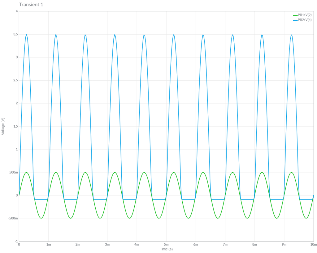
This graph shows the relationship between input and output signals in your amplifier circuit:
Input signal (green line labeled PR1(2)):
- Shows a sine wave with 0.5V peak amplitude (ranges from -0.5V to +0.5V)
- Completes 10 cycles in 10 milliseconds, confirming the 1kHz frequency
- Centered at 0V (no DC offset)
Output signal (blue line labeled PR2(4)):
- During positive input: Output peaks at approximately 3.5V
- During negative input: Output clips at approximately 0V (cannot go negative)
- Maintains the same 1kHz frequency as the input
Key observations:
- Amplification: When input is positive, gain is approximately 7× (0.5V → 3.5V)
- Single-supply limitation: When input goes negative, output cannot follow because:
- The op-amp’s VS- is connected to ground (0V)
- The output cannot go below ground without a negative power supply
- This creates the flat-line clipping at 0V during negative input cycles
- Precise timing: The output peaks exactly when input peaks, showing no phase shift
This graph clearly demonstrates both the amplification capability and the limitation of a single-supply op-amp circuit when handling bipolar (positive and negative) input signals.
19. What does “10 cycles in 10 milliseconds” tell us about frequency?
Frequency is the number of complete cycles that occur in one second, measured in Hertz (Hz). We can calculate it using:
Frequency = Number of cycles ÷ Time in seconds
In this graph:
- The horizontal axis shows time from 0 to 10 milliseconds (0.01 seconds)
- We can count exactly 10 complete up-and-down cycles in this time period
Calculation:
- 10 cycles ÷ 0.01 seconds = 1000 cycles per second = 1000 Hz = 1 kHz
You can verify this by measuring a single cycle:
- Each complete cycle takes exactly 1 millisecond (0.001 seconds)
- 1 ÷ 0.001 seconds = 1000 Hz = 1 kHz
This confirms that the signal frequency is 1 kHz, exactly matching the 1 kHz setting specified for the AC source (V2) in your circuit diagram. Frequency is one of the most important parameters of an AC signal because it determines how rapidly the signal changes – critical in audio applications where frequency corresponds to pitch.
20. Why does the output signal go slightly below zero?
You’re absolutely right – looking closer at the graph, the blue output line (PR2(4)) does go slightly below 0V, bottoming out at approximately -0.1V to -0.15V rather than exactly at 0V. This is an important observation that reveals real op-amp behavior:
Why the output goes slightly negative:
- Real op-amp limitations:
- The LM358 can’t typically swing all the way to the negative rail (VS-)
- But it can sometimes go slightly below ground (by about 0.1-0.2V)
- This is called “output saturation voltage” in datasheets
- Technical explanation:
- Inside the op-amp’s output stage are transistors that can’t fully turn on/off
- When trying to pull all the way to ground, the output transistors reach saturation
- This creates a small voltage drop of about 0.1-0.2V
- Practical implications:
- This behavior is actually beneficial in single-supply applications
- It allows the op-amp to reproduce slightly negative portions of input signals
- However, it can’t go significantly negative without a negative power supply
This slight ability to go below ground is one reason the LM358 is popular for single-supply audio applications – it can reproduce a tiny bit of the negative portion of the waveform, reducing distortion.
21. How is a negative output voltage created in a single-supply op-amp?
The slightly negative output voltage is created by a specific interaction of transistors in the op-amp’s output stage:
- Output stage structure:
- The LM358 output stage contains complementary transistors arranged in a “Class AB” configuration
- The “pull-down” side uses NPN transistors that connect to ground
- These transistors are designed to sink current (pull the output down)
- What happens during saturation:
- When the input signal goes negative, the op-amp tries to drive its output as low as possible
- The internal transistors turn on fully (saturate) to pull the output down
- During this saturation, the internal transistor junction capacitances store energy
- The mechanism creating negative voltage:
- When the transistors rapidly change states, this stored energy discharges
- This creates a small “undershoot” or “overshoot” below ground
- This effect is similar to how inductive “kickback” works in other circuits
- The output briefly goes negative (to about -0.1V) before settling
- Contributing factors:
- The specific behavior of the LM358’s output stage design allows this undershoot
- The load connected to the output (in this case R1) interacts with this effect
- Some op-amps specifically include this capability as a design feature
This slight negative capability is actually beneficial in many audio and signal processing applications, as it reduces distortion when handling signals that cross zero volts.
Conclusion
This non-inverting amplifier circuit demonstrates how op-amps create controlled amplification through feedback resistors. The LM358’s behavior shows both ideal amplification characteristics and real-world limitations, providing valuable insights for practical electronic design.
Note: This article was created with AI assistance.